Content
Flex Interface Board for a Satellite Communications System
In this project a flex interface board was designed. It will be used in a satellite communication system. The board has two high speed aerospace graded connectors, high speed differential and SPI interfaces. On the flex part of this PCB the traces were routed between ground planes so that the influence of space EMI will be at a minimum. Figure 1 highlights the specific shape of the PCB so that it will integrate smoothly with other sub-components of the satellite communications system.

Figure 1. PCB 3D Bottom View.
Input Testing Board for a Satellite Communications System
In this project a test board for a satellite communication system was designed. As was presented in the project above, the satellite communication system consists of a flex board with high speed differential signals and input-output connectors. As can be seen in Figure 1 there are several interfaces: three high speed differentials and two SPI interfaces that are driven at the highest possible clock speed. There are six SMA connectors and three standard headers. There are two conditioning ICs and one power connector. In the middle, but on the bottom side, as can be seen in Figure 2, there is the main output connector, that is a high speed aerospace graded connector. This PCB is a four layer FR4 board.
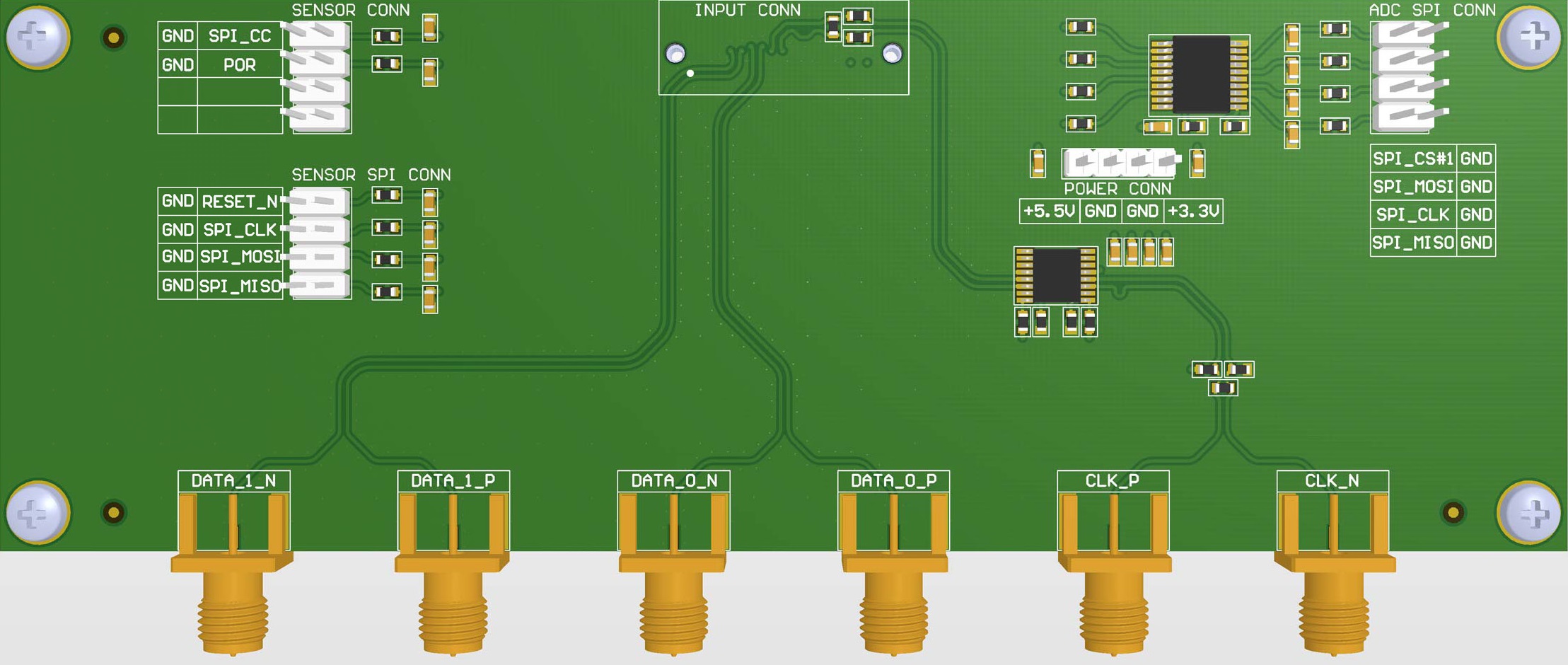
Figure 1. PCB 3D Top View.
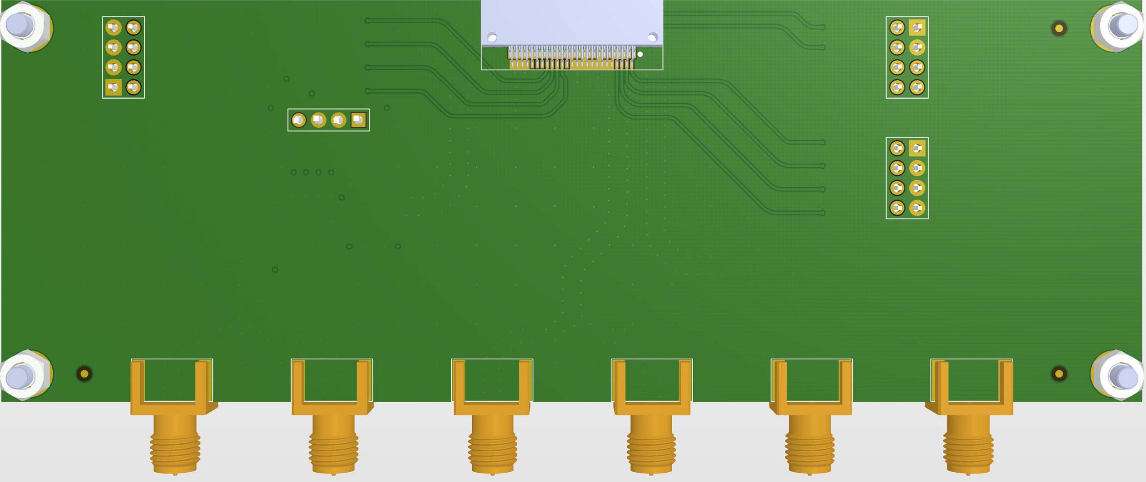
Figure 2. PCB 3D Bottom View.
Controller and Communications Board for an Electrical Vehicle Charging Station
In this project a complex board for monitoring the power delivered to an electrical car was design. This board is part of an electrical vehicle charging station. As can be seen below this board had many iteretions. Each one was enhanced and improved until the last revision that can be seen in Figure 9. This board represents the state of the art in monitoring the input power, that is delivered by an electrical changing station to an electrical vehicle.
The first version of the board, that can be seen in Figure 1, has an AC/DC power supply, a main controller for monitoring the voltage and current consumed and a double header for a WIFI module. The main controller compute localy the power consumed and the WIFI module send the instantaneous values to a remote server. This version and all the versions until V5I3 were designed to monitor the power consumed for 1 phase of the system.
The versions from Figure 4 onwards were designed to monitor 2 phases of the system. In this way the power consumed was sampled and computed with a high degree of accuracy. As can be seen a second communications controller was used for backup and other functions. Also from version V5I9.1 that is shown in Figure 7 an Ethernet controller was fitted and the functionality of the board was extended. The latest version, that is highlighted in Figure 9 has the best communications modules on the market. These were chosen because they use the minimum power when transmitting and receiving and have the largest range when communicate the sampled data. Only the latest version of this board has fitted the J1772 EVSE+ controller. This one enhaces the functionality of the board by permiting a more robust control of the high voltage section and also a good communication with the control unit of the electrical vehicle charging station.
In Figure 10 the first version of the board can be seen. In Figure 11 this board is fitted in the enclosure that is part of the electrical vehicle charging station that is highlighted in Figure 13. In Figure 12 it can be seen the V5I7 version.

Figure 1. ZEF Controller Board V1I1 3D Top View.

Figure 2. ZEF Controller Board V3I1 3D Top View.

Figure 3. ZEF Controller Board V5I1 3D Top View.

Figure 4. ZEF Controller Board V5I3 3D Top View.

Figure 5. ZEF Controller Board V5I7 3D Top View.

Figure 6. ZEF Controller Board V5I8 3D Top View.

Figure 7. ZEF Controller Board V5I9.1 3D Top View.
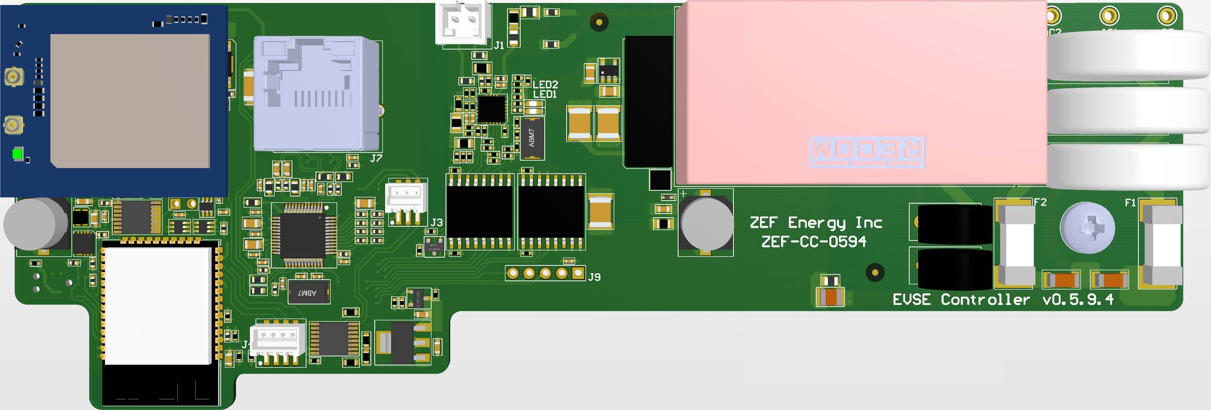
Figure 8. ZEF Controller Board V5I9.4 3D Top View.
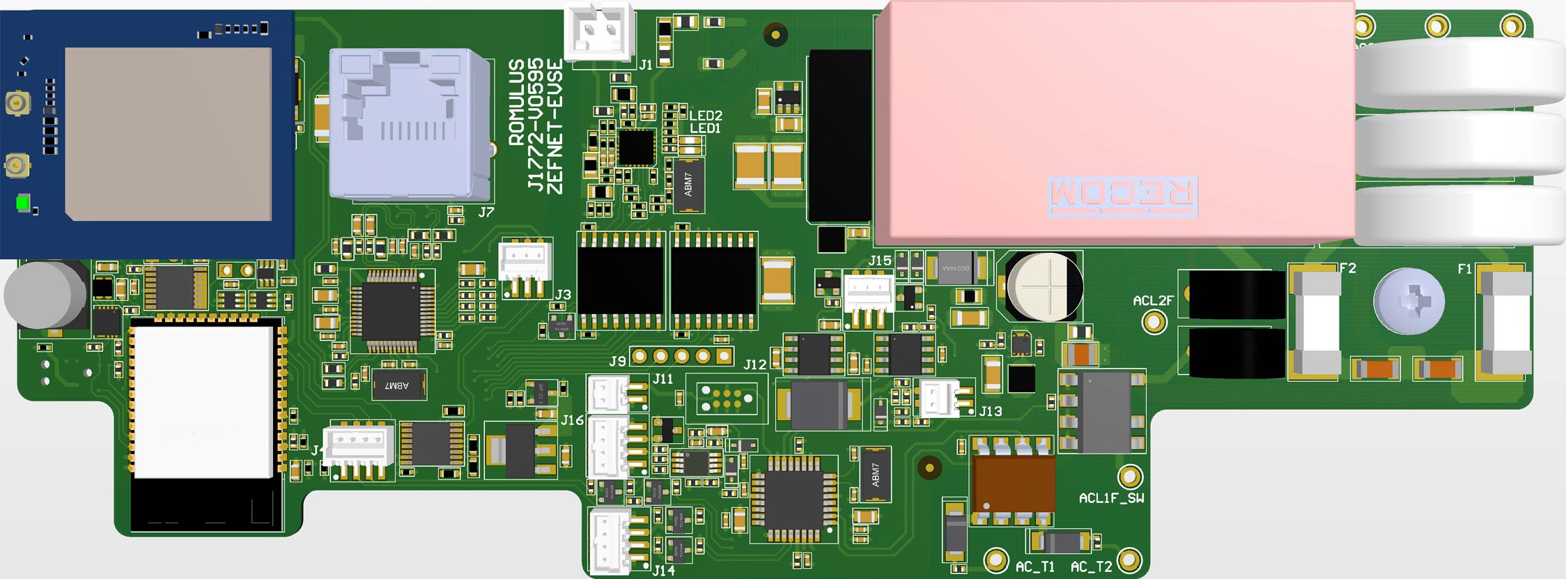
Figure 9. ZEF Controller Board V5I9.5 3D Top View.
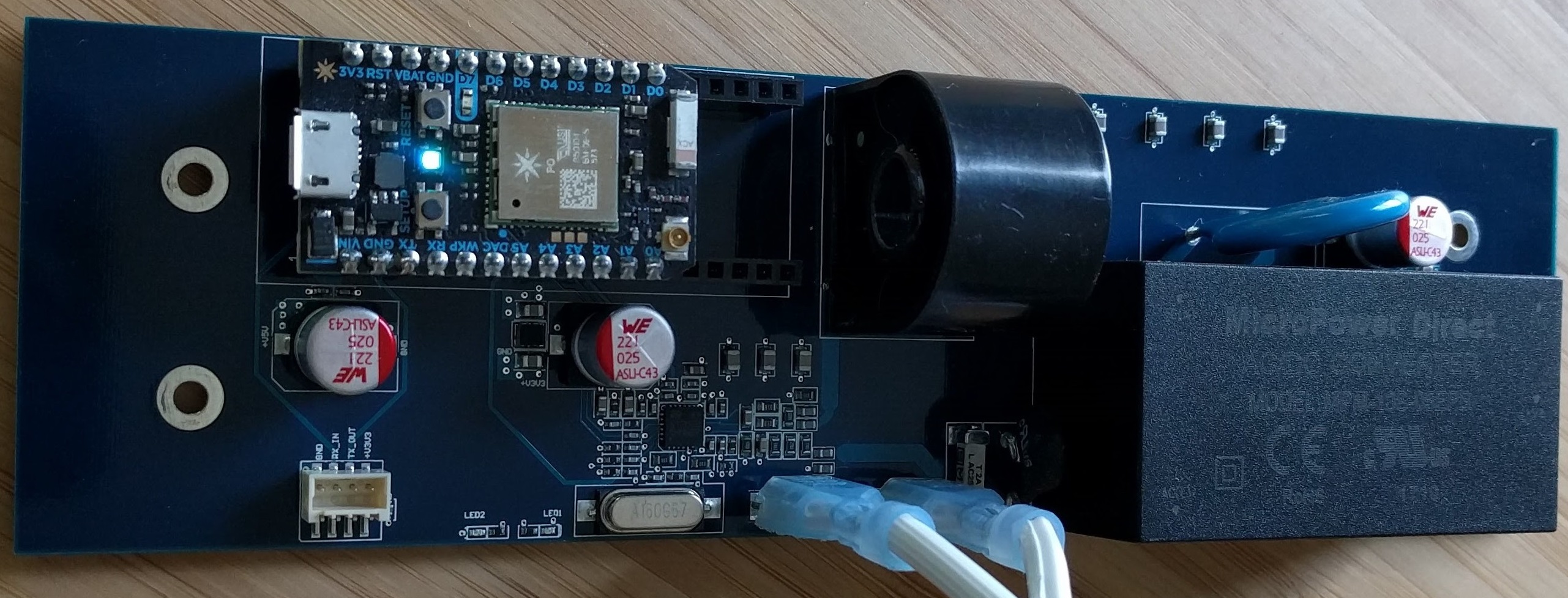
Figure 10. ZEF Controller Board V1I1 Real Board.
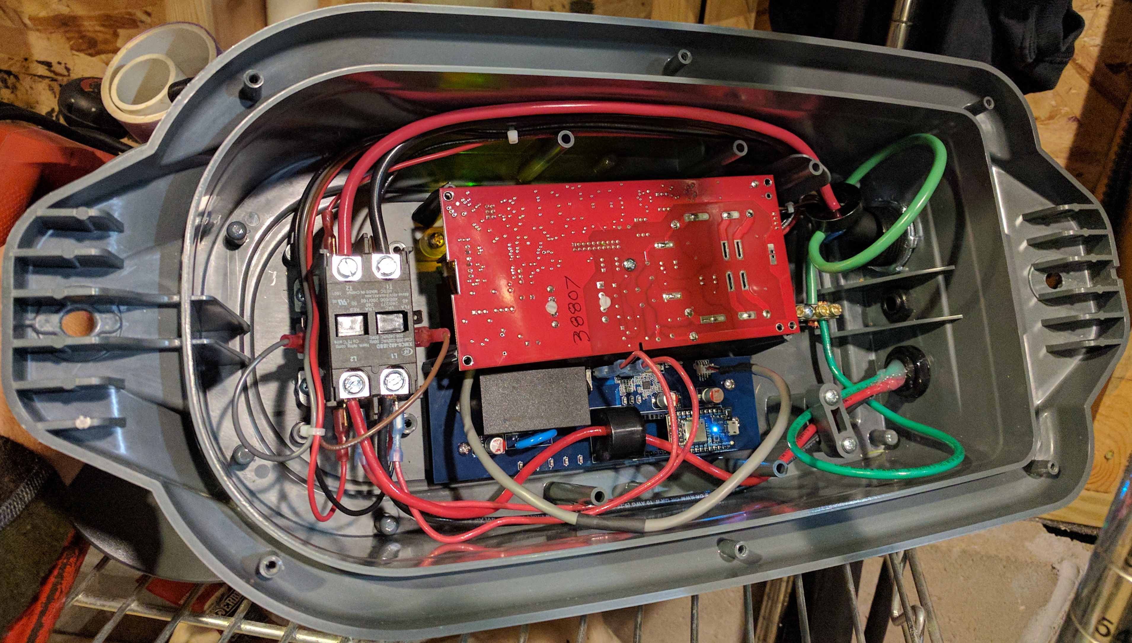
Figure 11. ZEF Controller Board V1I1 in Enclosure.

Figure 12. ZEF Controller Board V5I7 Real Board.
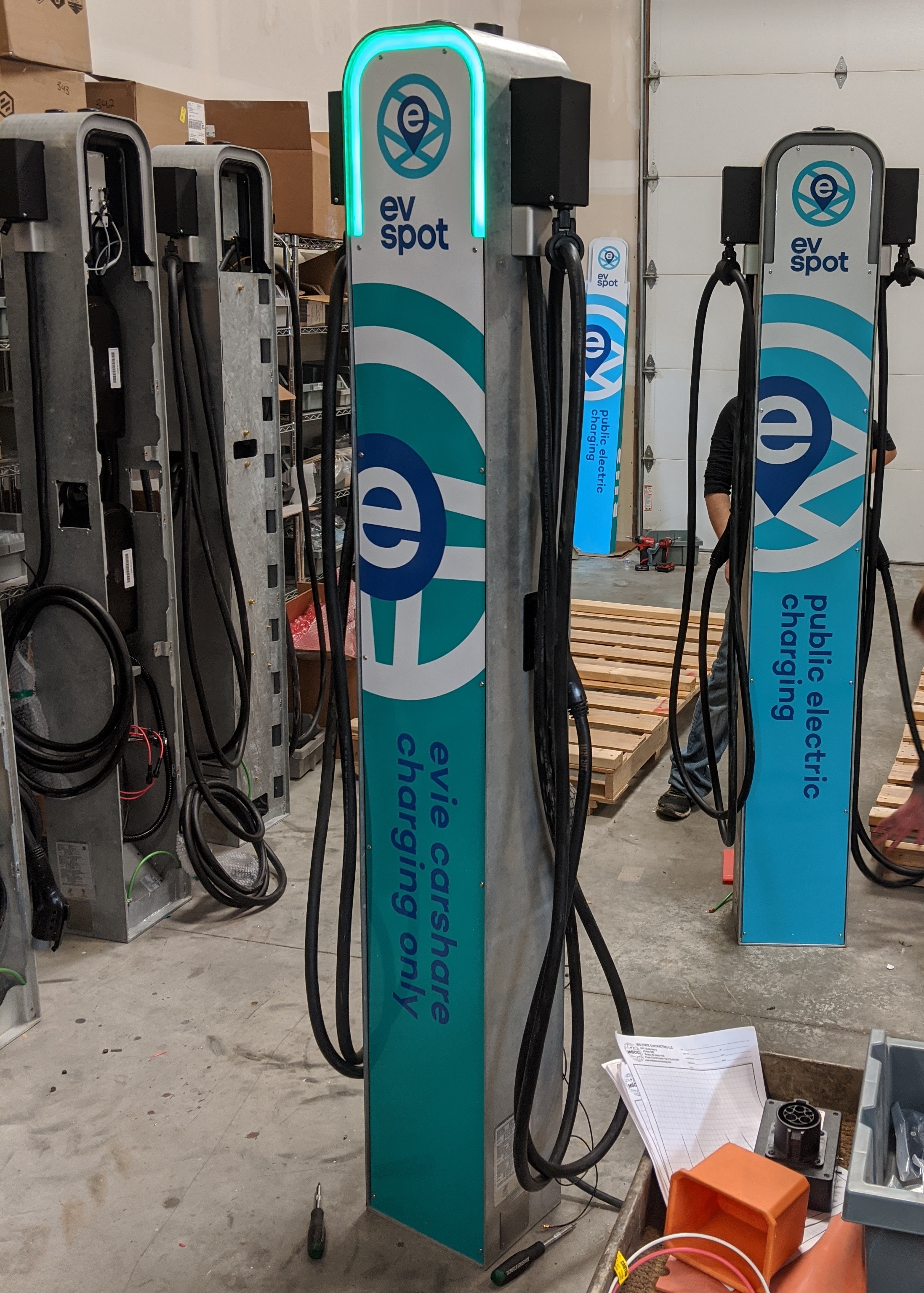
Figure 13. ZEF Electrical Vehicle Charging Station.
Controller Board for Monitoring Power Consumption of a House Located in a Harsh Environment
In this project a board for monitoring the power consumption of a house was design. Each component was chosen so that the board will work at lower temperatures such as -40 degrees Celsius.
The first iteration of this board has two versions. The difference between versions was the type of input power supplied and the circuitry to process it.
The first version has an AC/DC unit that receives 110 VAC and provides 12 and 5 VDC. After that a dual SMPS was used that receives 5 VDC and provides 3.3 and 1.8 VDC. Also there is a LDO that converts the 3.3 VDC into 2.5 VDC.
The second version receives 24 VAC and uses a rectifier unit to output 24 VDC. After that two SMPS were connected in cascade. The first one receives 24 VDC and provides 12 VDC, then this output is used as the input for the second SMPS to ouput 5 VDC. Again the same SMPS and LDO configuration was used to convert the 5 VDC into 3.3 and 1.8 VDC and 3.3 VDC into 2.5 VDC.
Both versions have a four channel Analog to Digital converter unit that samples the voltage, current and ambient temperature and send them to a control unit through SPI interface. There are also four 12 VDC relay units actuated by the same control unit. Each board provides some visual status using an RGB LED. Also on each board can be found a controller for a 1-Wire Slave interface. Both boards have a 2 to 1 Hub USB controller. The main control unit is a SODIMM Raspberry Pie.
The second iteration of this board has also two versions. Again the difference between versions was the type of input power supplied and the circuitry to process it.
The first version has an enhanced AC/DC unit that accepts a wide range of input voltages from 115 VAC to 230 VAC and outputs 12 VDC. After that two SMPS were used in parallel to receive the 12 VDC and provide 5 and 3.3 VDC.
The second version has a rectifier unit that receives 12 VAC and an SMPS to process this and provide 12 VDC. As in the first version there were used two SMPS in parallel that received the 12 VDC and provided 5 and 3.3 VDC.
Both boards have four relay sensing units so that the it will be more robust. The RGB LED was replaced by nine single LED circuits that provide relay and system visual status. The 1-Wire Slave interface was fitted with a I2C level shifter so that it will be compatible with the new control unit. The main control unit is a Photon/Electron Board. The main asset of these two versions is the power measuring controller unit, that accurately measures the input voltage and current and provides the exact power consumed of the appliances in the house.
Both iterations have the ability to buffer the computed consumed power for a period of 30 days and could send those values to a remote monitoring server each day or once a month.
Figures 1 through 4 show the 3D view for both variations and for both versions of the board. Figure 5 through 7 highlight the real pcb and its use in a real live situation.
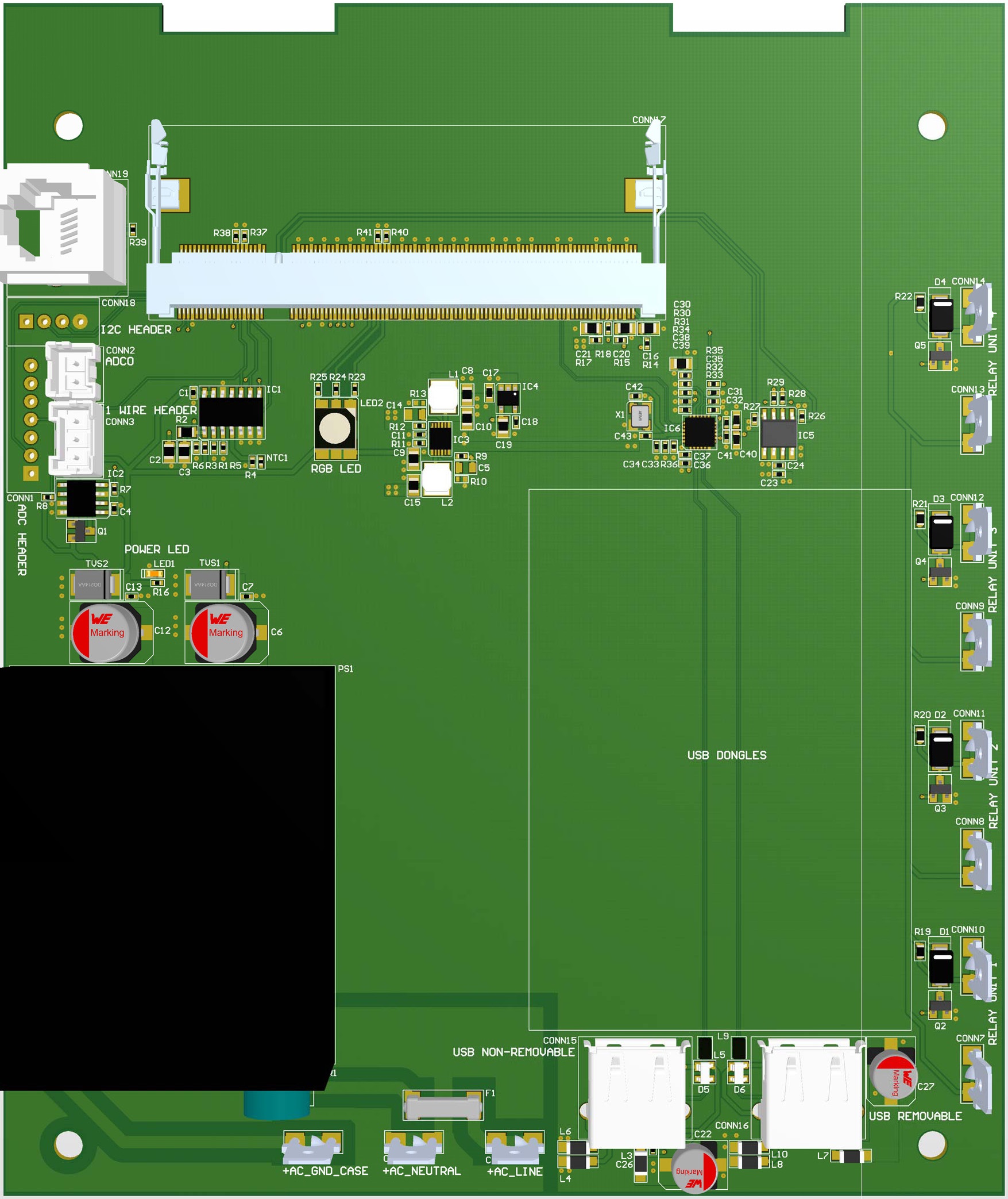
Figure 1. MSU PCB 3D Top View for V1I1 First Variation.
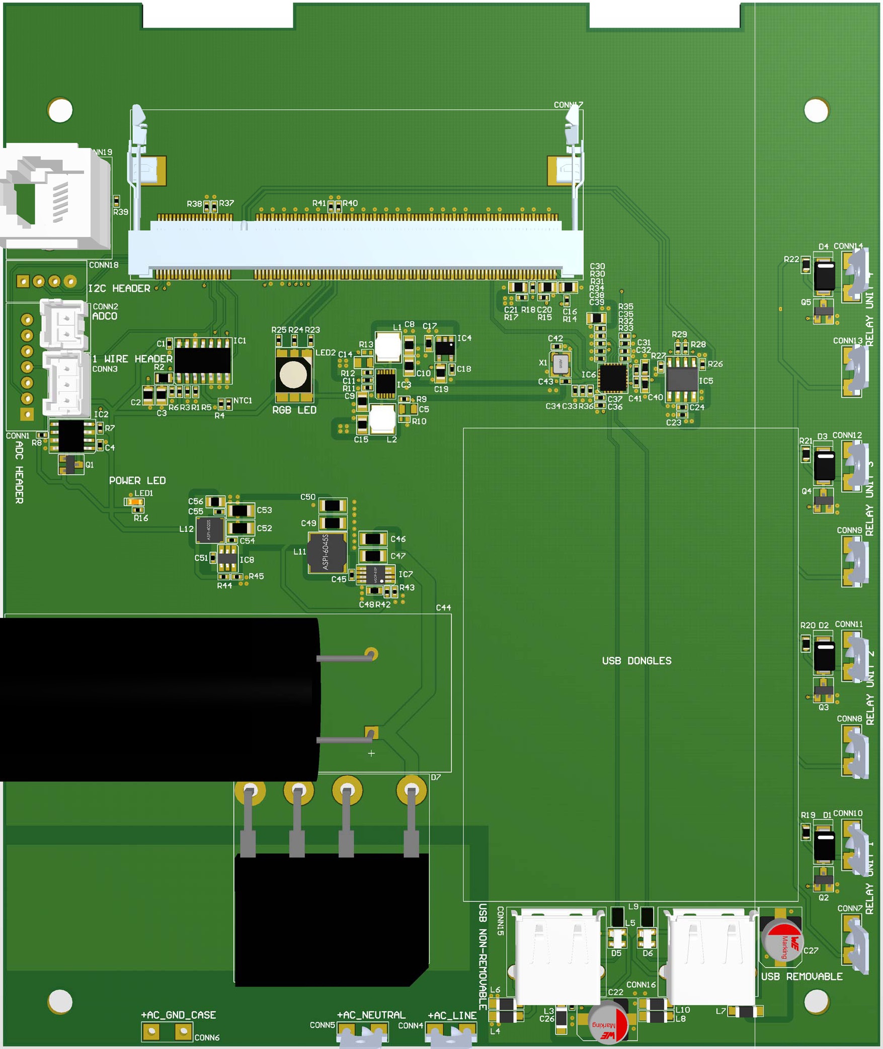
Figure 2. MSU PCB 3D Top View for V1I1 Second Variation.
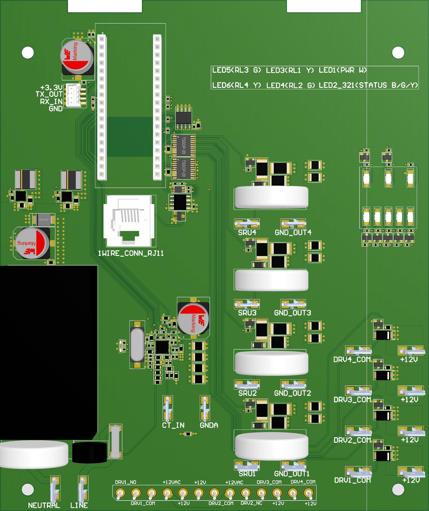
Figure 3. MSU PCB 3D Top View for V1I2 First Variation.

Figure 4. MSU PCB 3D Top View for V1I2 Second Variation.
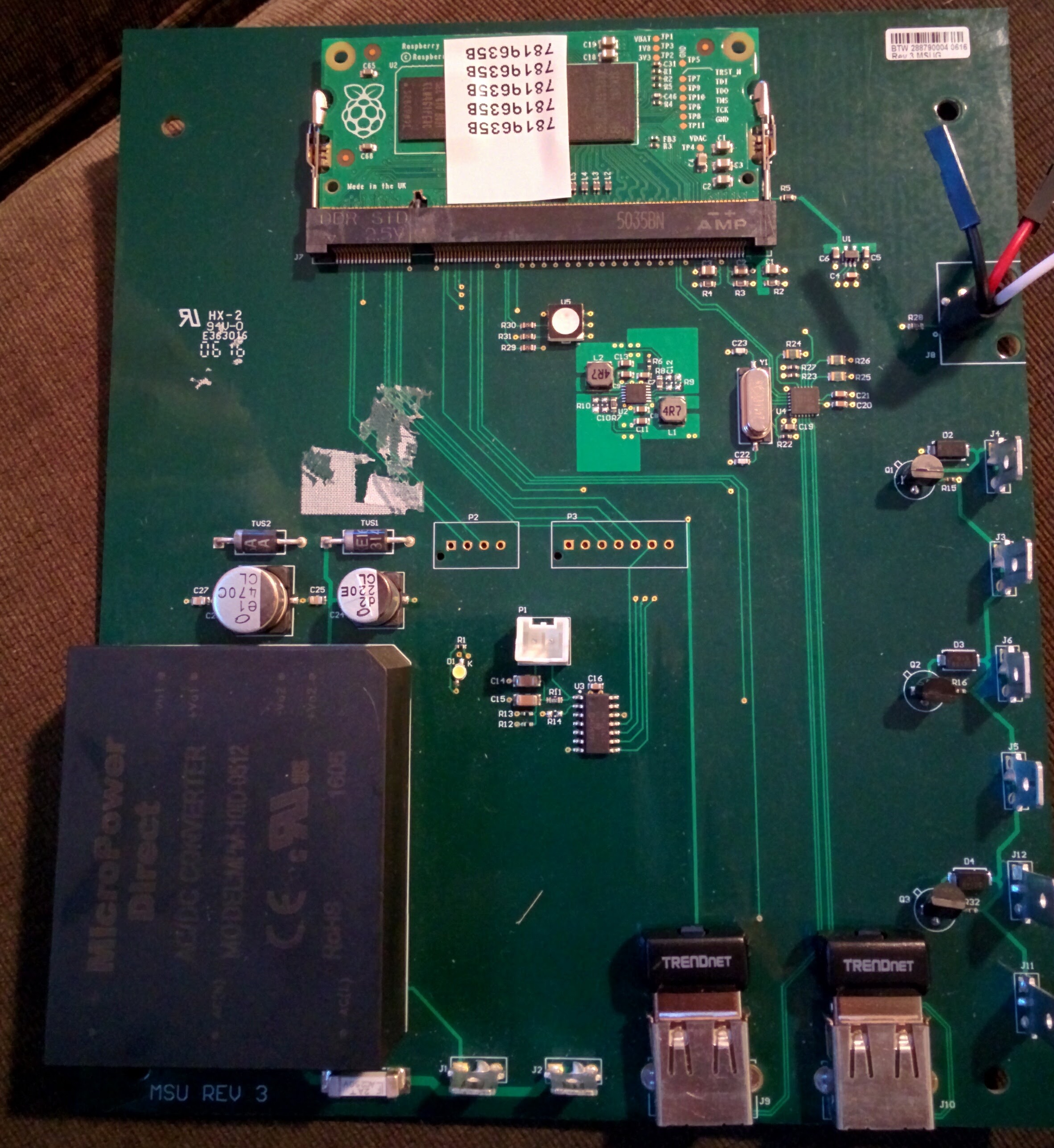
Figure 5. MSU PCB Real Board 1.
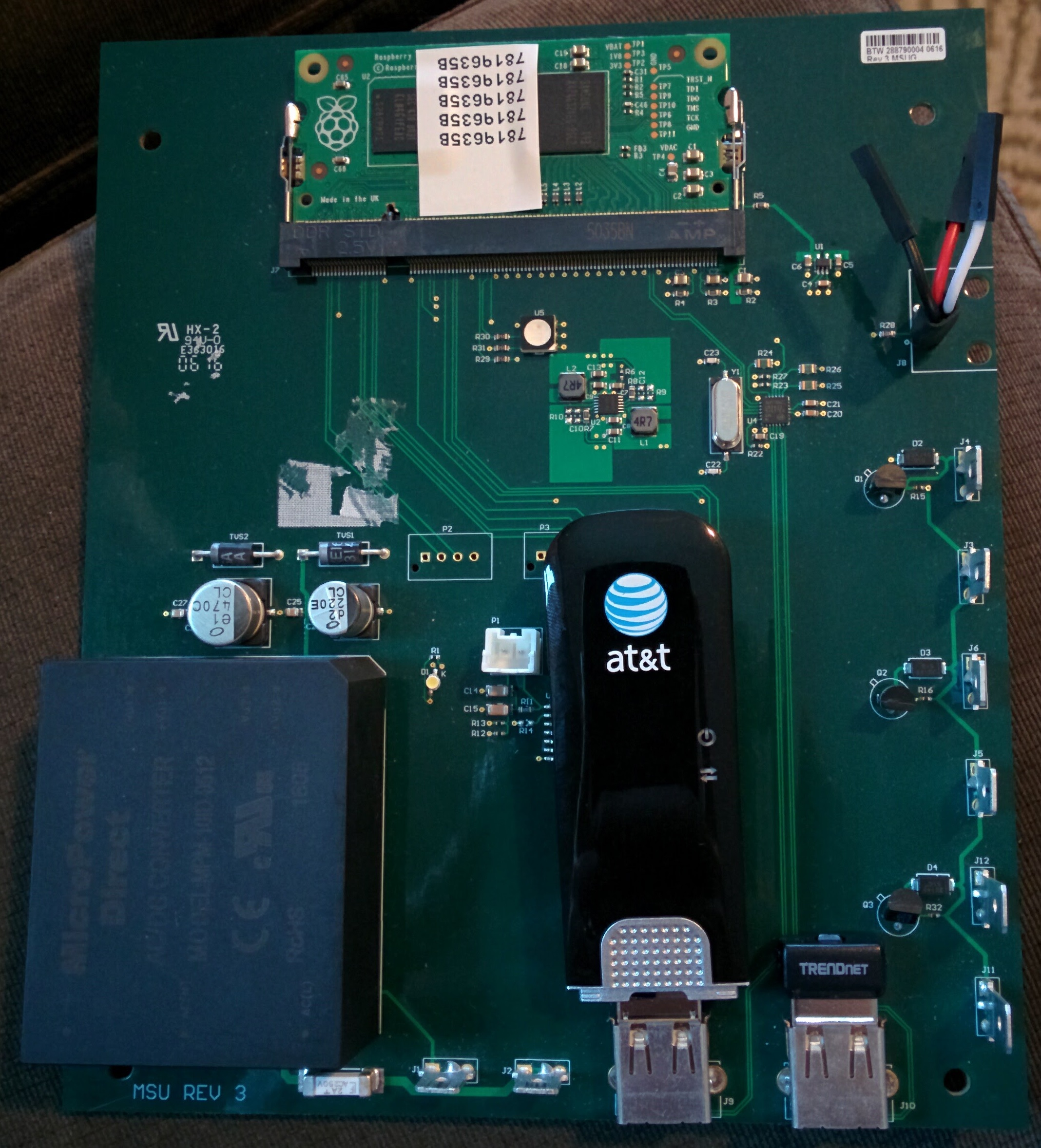
Figure 6. MSU PCB Real Board 2.
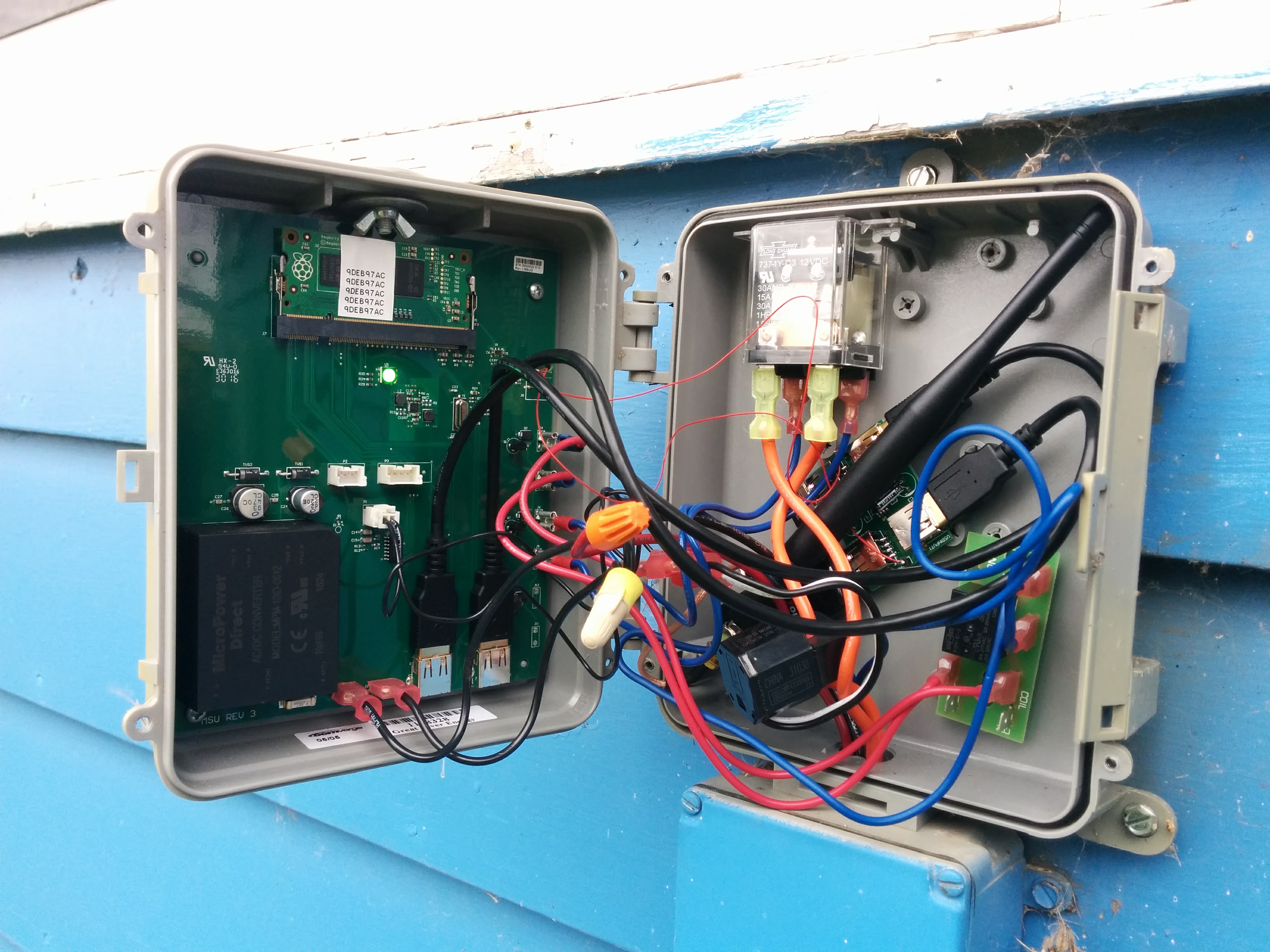
Figure 7. MSU PCB Real Board 3.
Dual Smart Card Reader
The circuit shown in Figures 1, 2 and 3 is used in the food and beverage industry for paying the products. The complete system is shown in Figure 4. The Dual Smart Card Reader is based on the Microchip Smart Card Chip SEC1210 which has USB and SPI interfaces. The board can be powered from a 5 V barrel connector or an USB2 interface. The input power can be automatically selected using a power multiplexer. The board is equipped with two smart cards. One is a SIM card from Amphenol and the other is a 2FF Mini SIM card from TE. The board has also an SPI to UART interface chip. Utility headers were used for SPI, UART and power interfaces.
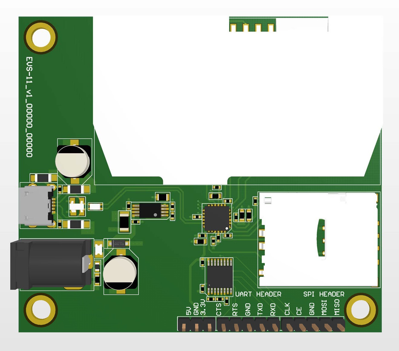
Figure 1. Dual Smart Card 3D Top.
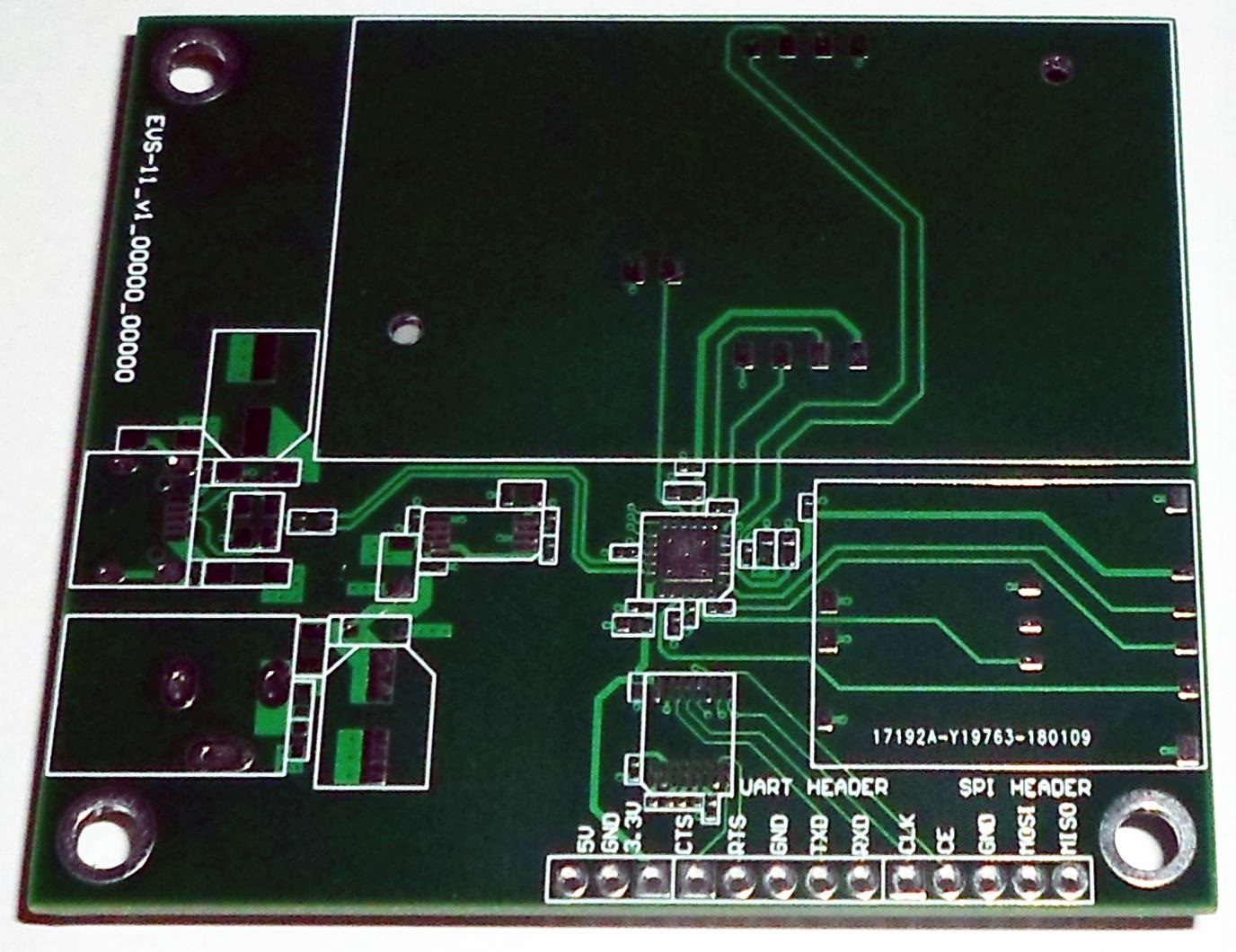
Figure 2. Dual Smart Card Unpopulated Real Board.
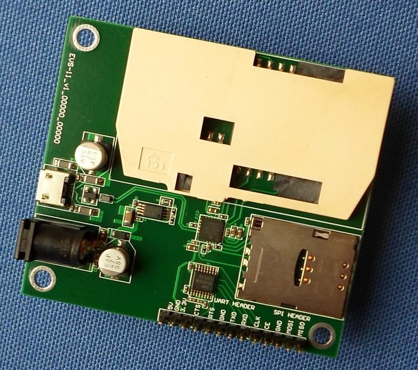
Figure 3. Dual Smart Card Populated Real Board.
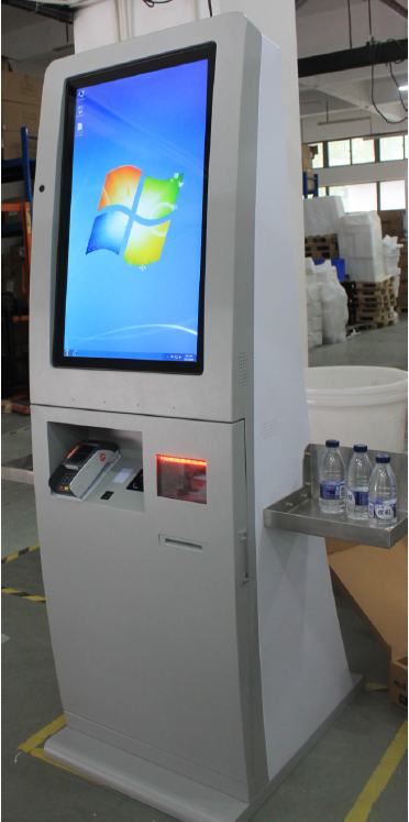
Figure 4. Dual Smart Card Enclosure.
Audio MEMS Sub-module
The circuit shown in Figures 1 through 4 is used in the food and beverage industry for giving feedback to the customer after ordering some products. The circuit works in conjunction with a Raspberry Pi 3 board which has installed an AI application. This setup can be seen in Figure 5. The Audio MEMS Sub-module is based on the ST ARM Cortex M3 Processor: STM32F107RCT6. The board can be powered from a 5 V barrel connector or an USB2 interface. The power to the board can be automatically selected using a power multiplexer. The board is equipped with a USB2 COM compliant circuitry. The processor can be programmed using a 6 Pin Tag-Connect no legs connector. It has 4 MEMS microphones: two for left side and two for right side. A 40 pin connector header was used for interfacing this board with the Raspberry Pie 3.

Figure 1. Audio MEMS Sub-module 3D Top.

Figure 2. Audio MEMS Sub-module 3D Bottom.

Figure 3. Audio MEMS Sub-module Top Real Board.

Figure 4. Audio MEMS Sub-module Bottom Real Board.
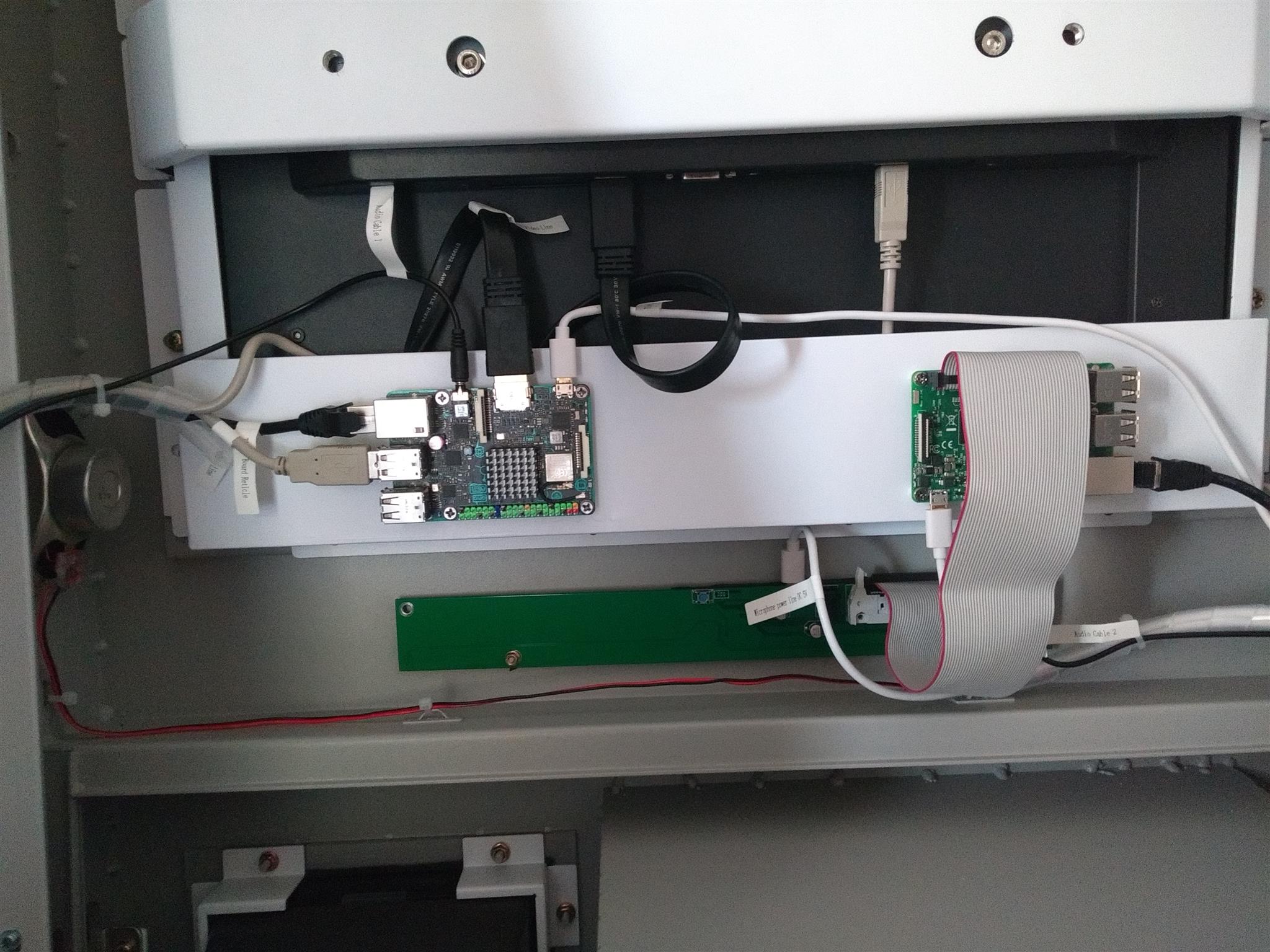
Figure 5. Audio MEMS Sub-module Enclosure.
Smart Handle with High Speed Digital Interfaces for Future Fridges
In this project a complex board with many high speed digital interfaces was designed and implemented. Its 3D mechanical view is highlighted in Figure 3. The system has at its center the SolidRun SOM iMX8M Quad board, as can be seen in Figure 1. The smart handle board consists of various high speed interfaces and the corresponding circuitry. The first ones are two USB2 and two USB3 interfaces highlighted in Figure 1. One USB2 controls a Quectel BG96/EG91 LTE SOC module and the other USB2 and an USB3 are used in conjunction with a 4 port USB3 HUB controller that communicates with an Opticon barcode scanner, a cVend payment module, an Omron face and human detection camera and the last USB interface was left free for future behavior integration. Another high speed interface is the HDMI that will be used to connect the smart handle board with an LCD monitor, also shown in Figure 1. The board has incorporated a NFC PN7150 reader, as can be seen in Figures 2 and 3. There is a high speed CSI camera interface and a MIPI-DSI interface for a TFT display. The last two interfaces are a PCIe interface for an SSD memory card, as can be seen in Figure 2 and an Ethernet interface for internet connectivity, as can be seen in Figure 1.
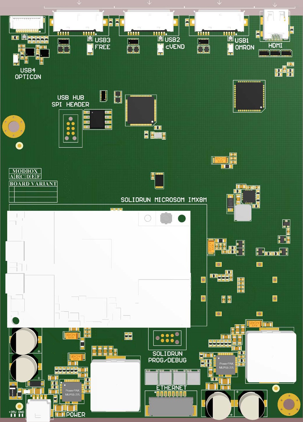
Figure 1. Smart Handle 3D Top.
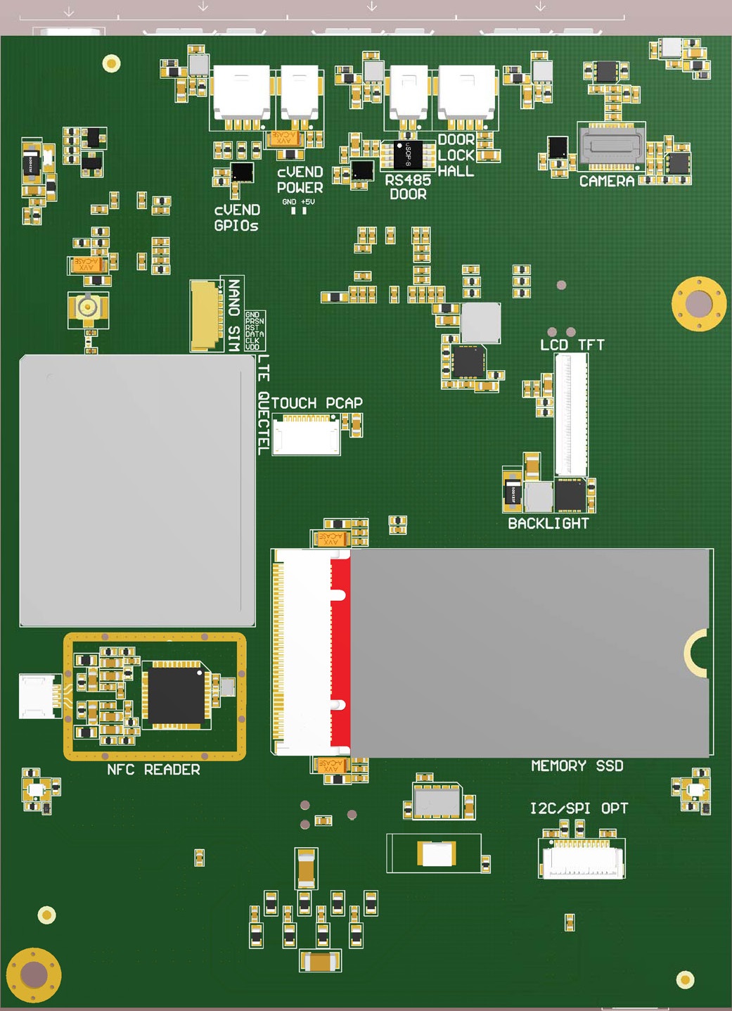
Figure 2. Smart Handle 3D Bottom.
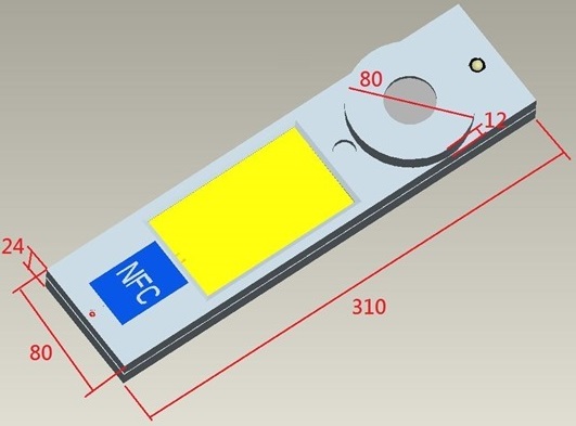
Figure 3. Smart Handle 3D Mechanical.
Complex Interface Board with High Speed Peripherals
Figures 1 and 2 show a complex mixed signal board that consists of many interfaces like: RS232, MicroSD, Ethernet PoE+, USB, RFID, Display and Touch Sensor, Audio and HDMI. In Figure 3 can be seen the enclosure and the board fit within it. This is a Modular Display System and all the high speed peripherals are controlled by the SolidRun SOM iMX8M Quad board that is the heart of the system, which can be seen in the upper left part of Figure 1.
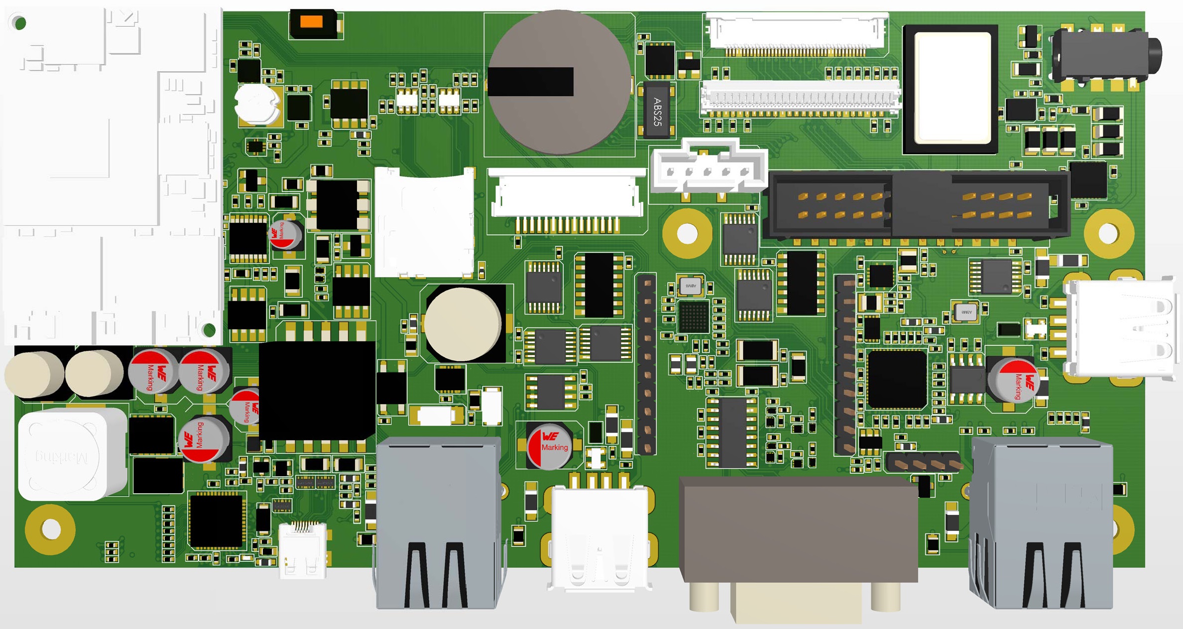
Figure 1. Complex Interface 3D Top.

Figure 2. Complex Interface Top Real Board.
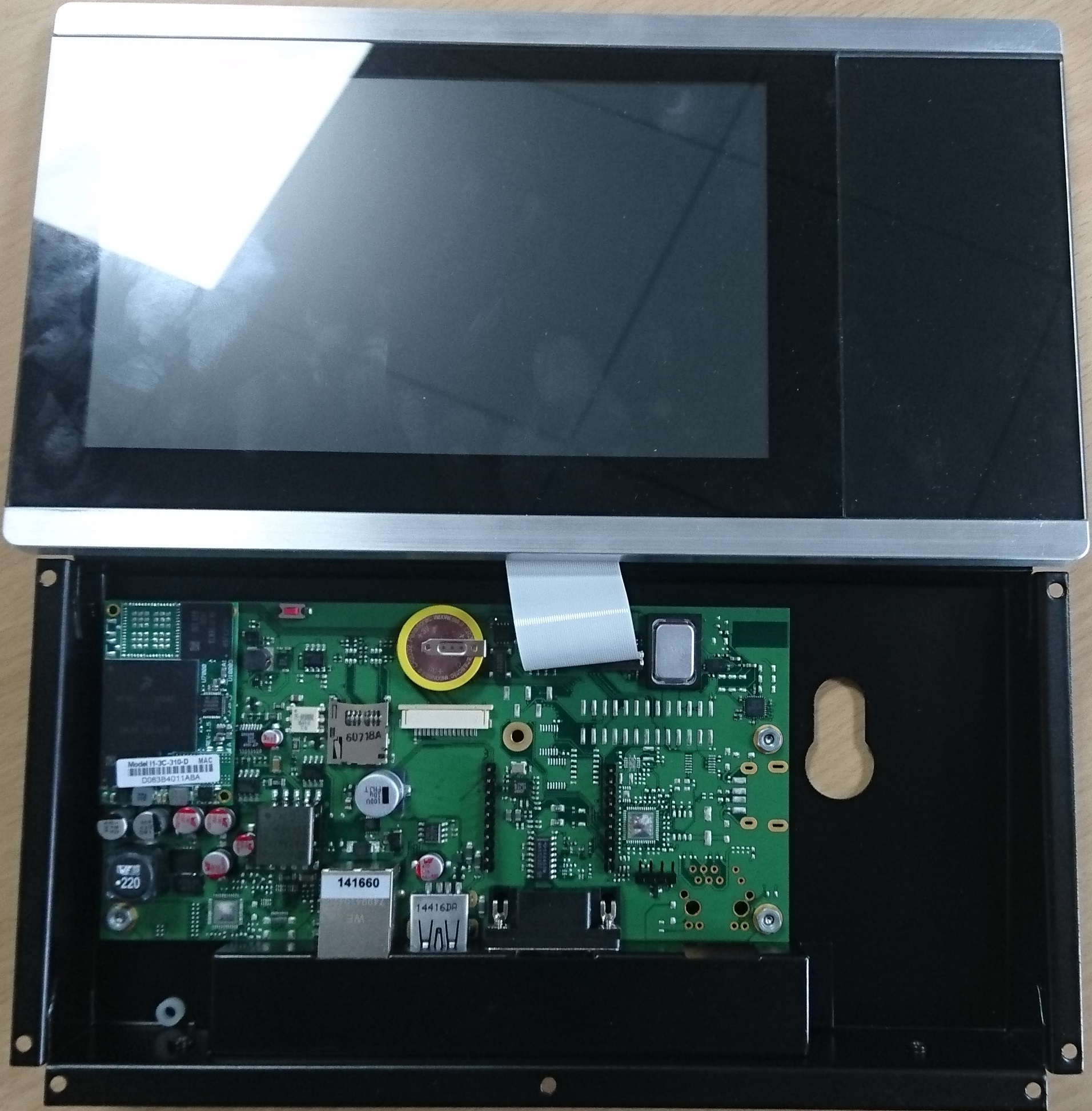
Figure 3. Complex Interface Board Enclosure.
BLDC Motor Controlling Boards
The project consists of two boards. The first board named the Main Controller is highlighted in Figures 1 and 2 and has an ARM processor named STM32F100VCT6B. The second board named the Motor Controller is highlighted in Figures 3 and 4 and has an ARM processor named STM32F103CBT6. The user sends commands through the USB. The Main Controller has a mini USB2 type B connector. The USB data packets from and to the user are processed by an FTDI chip named FT232H which is the bridge between the user and the ARM processor on the Main Controller. This ARM processor communicates with the second ARM processor which is on the Motor Controller through two FFC connectors sending and receiving information. The ARM processor on the Motor Controller actuates the BLDC motor using a motor driver CMOS parallel controller.
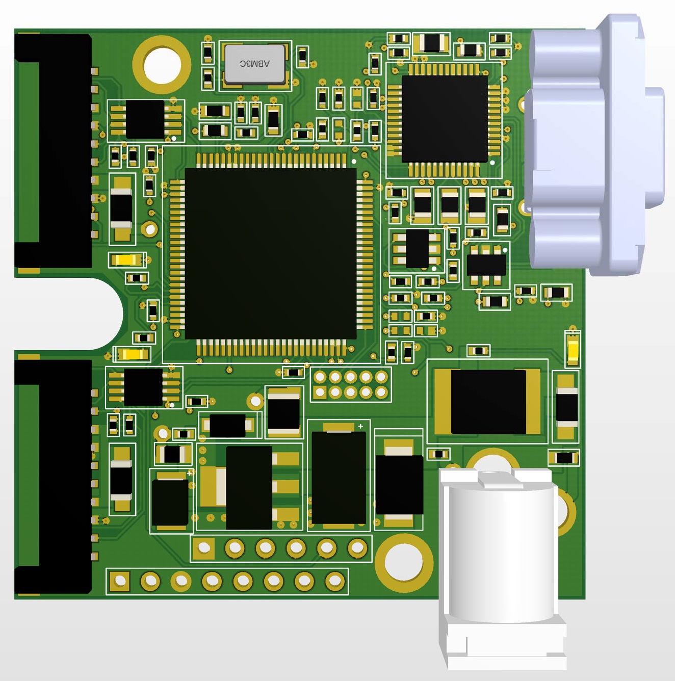
Figure 1. BLDC Main Controller Top 3D.
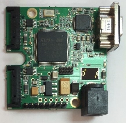
Figure 2. BLDC Main Controller Top Real Board.
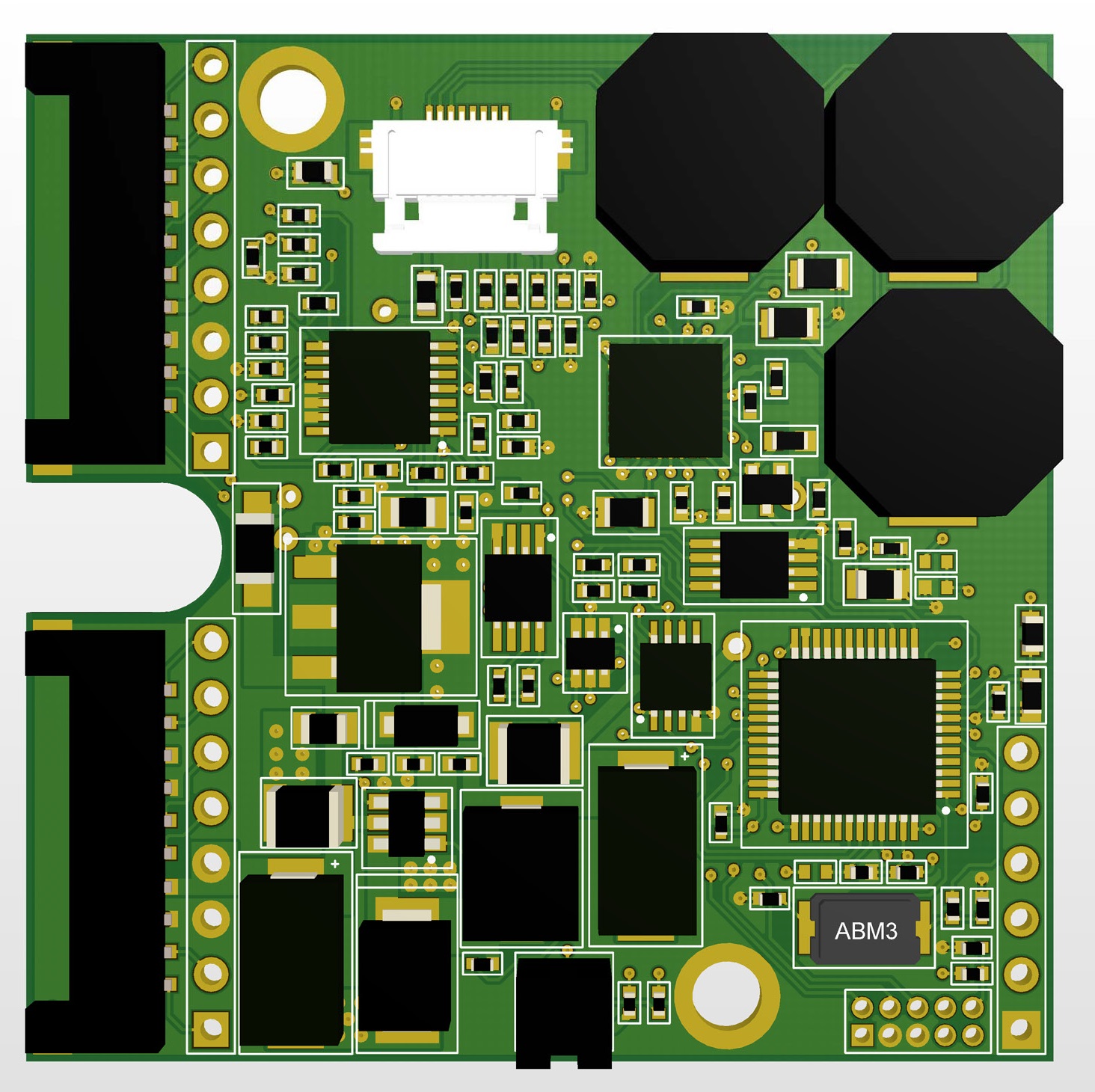
Figure 3. BLDC Motor Controller Top 3D.
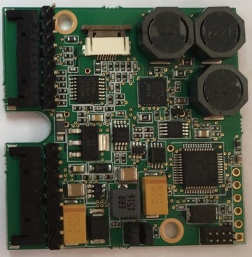
Figure 4. BLDC Motor Controller Top Real Board.
PID Controller Board for Laser Unit
Figures 1 and 2 show a PID Control Board for a Laser Unit. The board has an ARM processor from STM and two Analog to Digital Converters: one with 12 bits resolution, which is fitted and the other with 16 bits resolution that is not fitted. There is also a PT100 RTD temperature sensor. As can be seen in Figures 3 and 4 after the board was manufactured, it was fully tested and worked correctly.
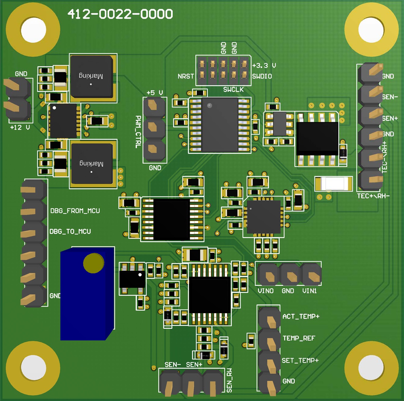
Figure 1. PID Controller Board for Laser Unit 3D Top.
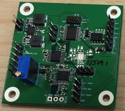
Figure 2. PID Controller Board for Laser Unit Real Board.
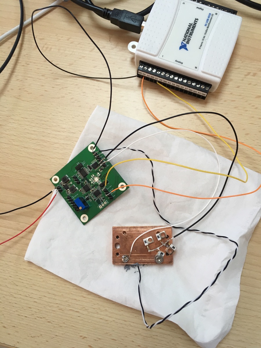
Figure 3. PID Controller Board for Laser Unit Testing.
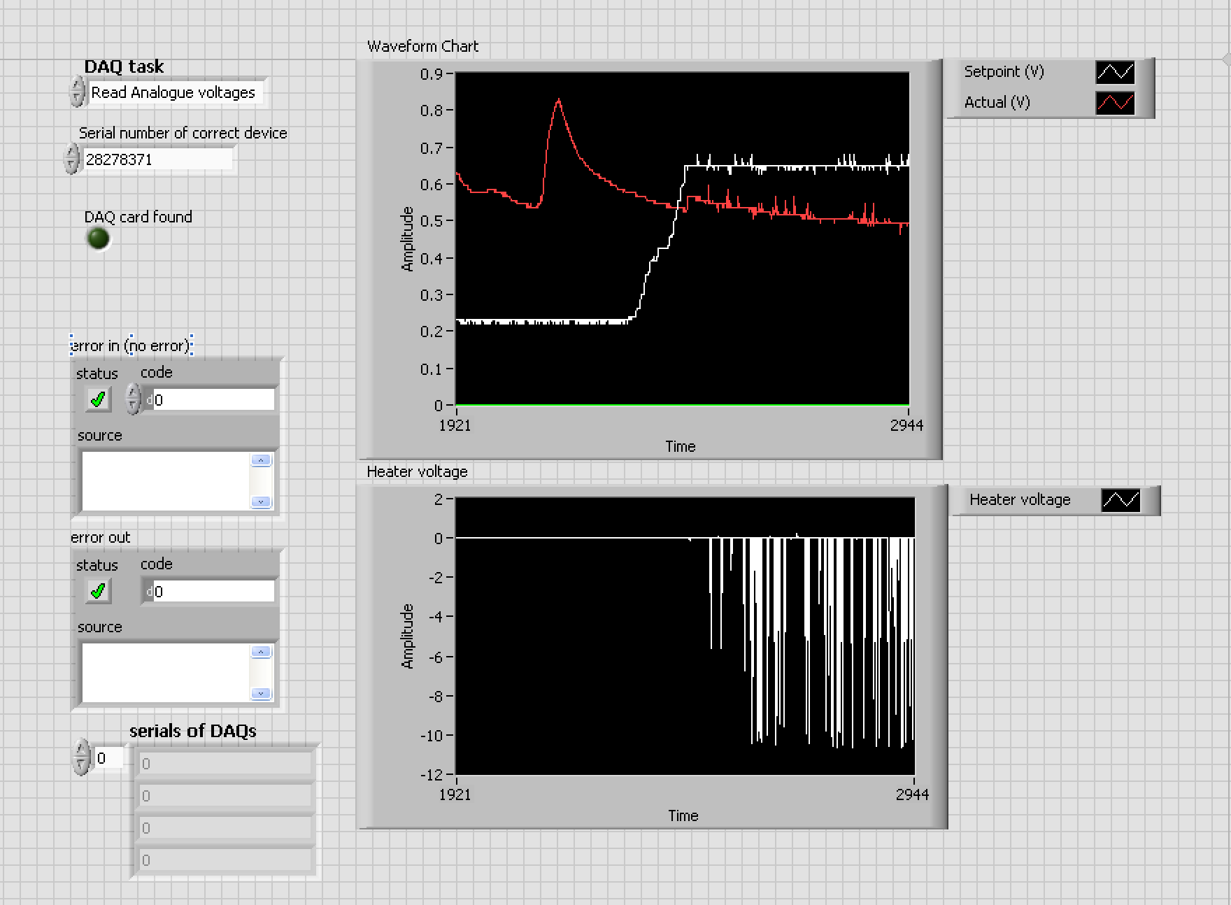
Figure 4. PID Controller Board for Laser Unit Software.
Advanced Microcontroller Board with FFC Peripherals
In this project a complex digital logic circuit was designed consisting of multiplexers, shift registers, I/O peripherals and an ATmega microcontroller. Three versions of this board are highlighted in Figures 1, 2 and 3. The installation, which was named Smart Floor Detection System, can be seen in Figure 4. There is a low frequency sensor surface and each band of sensors is connected to the main board through an FFC peripheral. One board has 8 I/O peripherals. The main board is connected in cascade with a copy of itself. The ATmega microcontroller buffers the acquired sensor data and communicates it with an Arduino board, as can be seen in the lower right of Figure 4. This project was done in collaboration with a post graduate student from MIT Media Lab.
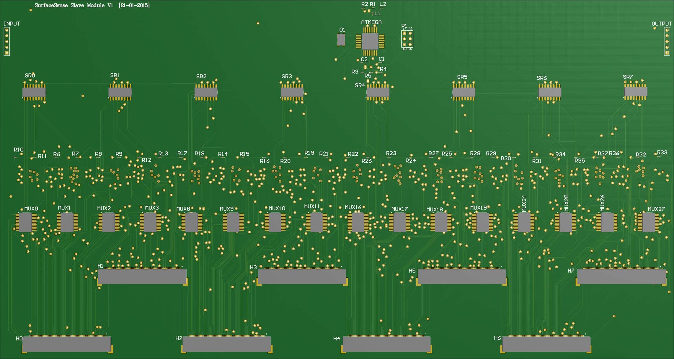
Figure 1. Advanced Microcontroller Board with FFC Peripherals V1I1 3D Top.
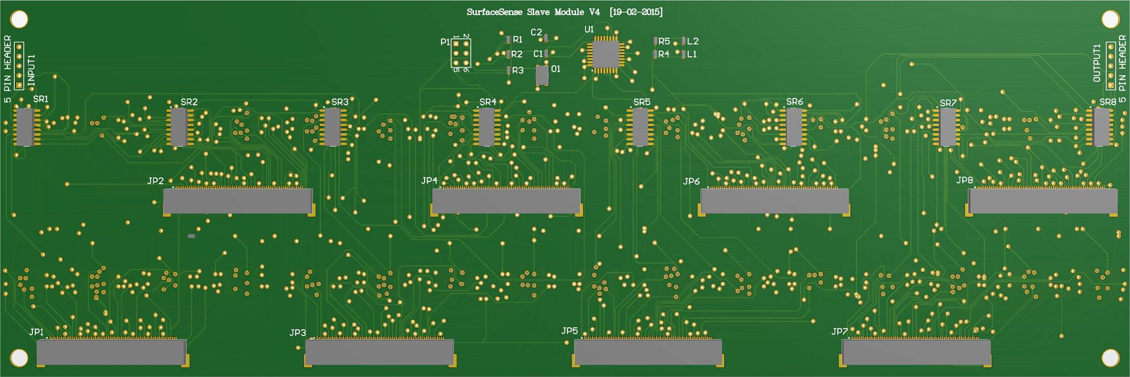
Figure 2. Advanced Microcontroller Board with FFC Peripherals V4I1 3D Top.
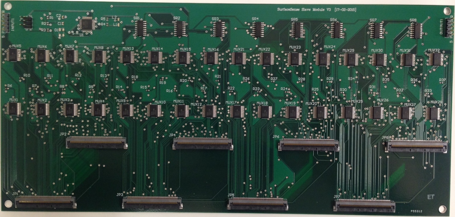
Figure 3. Advanced Microcontroller Board with FFC Peripherals V3I1 Real Board.
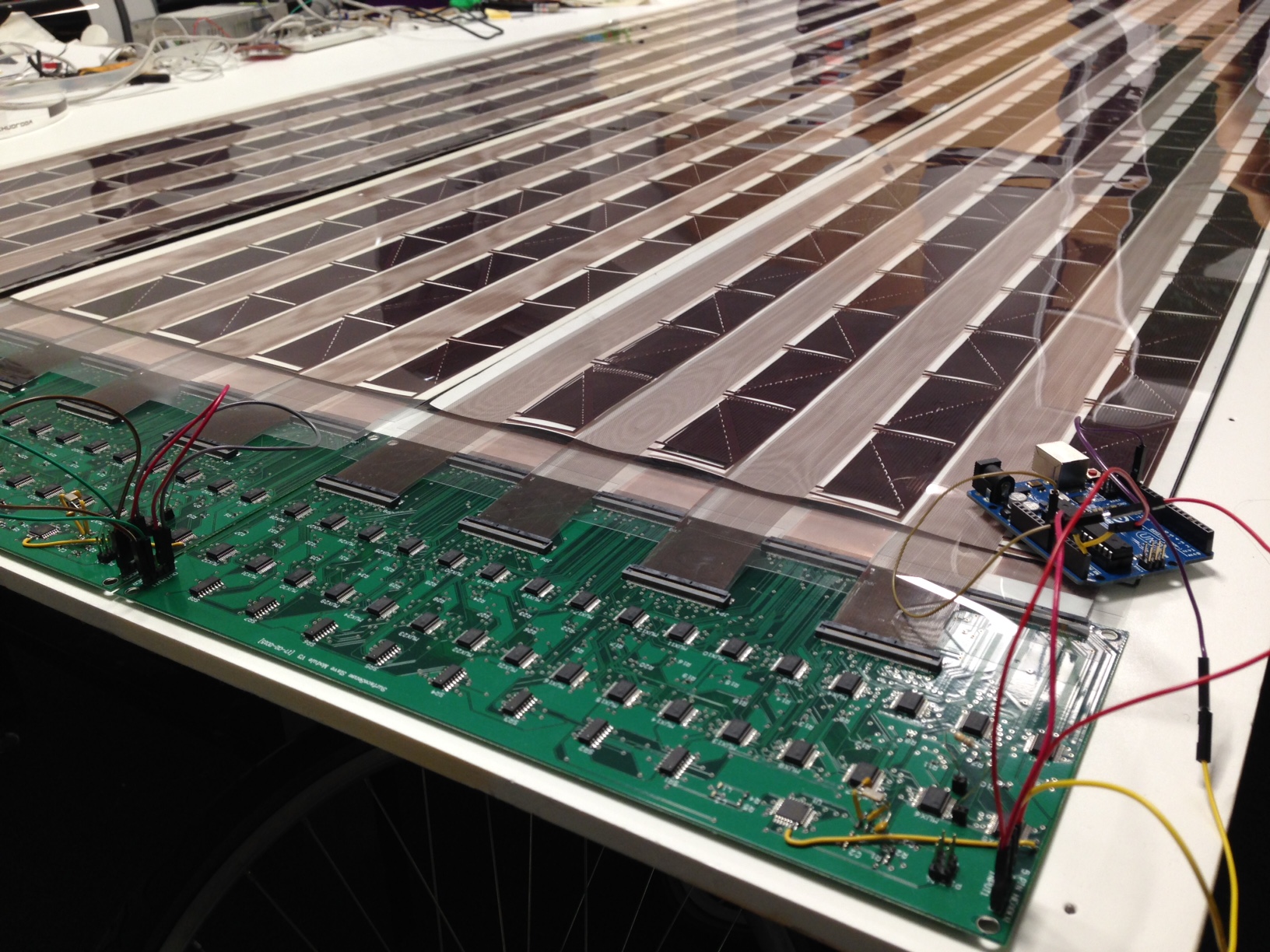
Figure 4. Advanced Microcontroller Board with FFC Peripherals V3I1 Testing.